
Back last spring and summer I was doing photography, and especially astrophotography. Well I eventually decided it was effecting my sleep cycle because in the summer you have to get up in the midnight to like 4am range for good dark skies. So I said “Wait till winter. It will be dark after dinner.”
But in the winter it is too cold! So instead of astrophotography I’ve been doing Ham Radio — which got to be a problem when I ran out of things to say on the radio, and so now I’m back on to electronics.
So I dusted of my Z80 computer design work, and redesigned it as a spiffy single board computer. One conundrum I had in last year’s design was that I did not want to set aside space for an EPROM, since I have no idea yet what sort of OS I was going to put on it, I had no idea how to size it. Many designs on the web just give it 16k or 32k of EPROM… which is huge.
But I stumbled upon a nifty chip… it’s a 128k NVRAM… what it is is low power, but pretty fast static ram with a built in lithium backup battery… So now that’s the best of both worlds… It will act like a ROM in that it will retain it’s memory when powered off, but I don’t have to know at hardware design time how much memory to set aside for the OS..
So I had panel switches in my design so I could manually “toggle” in a bootstrap program, to then pull in the OS off of something like an SD card, but instead what I decided to do was just make another board to program the NVRAM with a basic “ROM monitor”.
So I designed and, wow, already built a tiny Arduino compatible Atmega 2560 board to be the controller in the programmer. It was my first real SMD component board, and my first use of a cheap reflow oven I bought quite a while ago, but hadn’t used yet. The board is very basic, all it has on it is the 2560, a USB-UART chip, a 16mhz resonator. So very basic and also I brought out 16 pins, +5v, 3.3v, Gnd, 28 GPIO pins, and AREF (4 of the GPIO pins are also ADC inputs). Well I made the board key shaped so that the header pins are on an outboard portion of the board so that it is breadboard friendly — the 2560 is a big chip and would not normally fit on a board that fits on a breadboard.
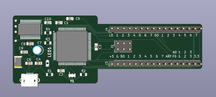
So 28 GPIO pins is exactly what I need to program the NVRAM chip… that’s 17 address lines, 8 bidirectional data lines, and 3 control lines (~CE, ~WE, ~OE).
Once built and debugged, I wrote a first version of the ROM monitor, but this one compiled for the 2560 and targeting the NVRAM chip. I can do only basic things… Examine and deposit individual memory cells, and, wow, I can also do Kermit file transfers for over the serial port file receives… So now I realized I don’t need panel switches on the Z80 board since it will have a Z80 compiled version of the monitor, which will also be able to pull in executables via Kermit.
And with about a days’s work, it worked! I did spend an additional earlier day trying to implement YMODEM, but found that protocol is not very well documented, and since Kermit is very well documented, and simple, I ultimately went with Kermit.
I built a version of the NVRAM programmer on a breadboard. It did work, but is just a mess of wires, and so it would be hard to remove and put back the NVRAM, or even the 2560 board– which I assume I’ll do as I develop the final monitor for the Z80…

You can see in this pic that the the 2560 board would normally cover all the pins on the breadboard, thus the key shape to allow room to plug wires onto the breadboard… the footprint is the same as a .1 by .6 pitch 32 pin DIP socket.
So I designed a PCB board for the task that I can plug the 2560 in and it has a ZIF socket for the NVRAM chip. Note those 3 resistors hanging out up at the top of the breadboard… Those are pull-ups on the 3 control lines… Since I am re-using the 3 SPI pins as GPIO pins, and the 2560 uses a combination of RESET and SPI to program itself, it’s pretty critical to not have anything active on the SPI pins during system RESET. Well the SPI pins landed as 3 of the data pins for the NVRAM chip… also one of the data GPIO is also for the onboard LED….. so the first time I powered it up I had a light show as the NVRAM chip had floating control lines it was doing strange things on it’s data lines, and the 2560 was struggling to figure out what sort of program was coming in to the chip. Adding pull-ups was all that was needed, the NVRAM chip now comes up with it’s data lines tri-stated.
OUCH! I actually made the same mistake when I sent the board out to have the PCBs made. I forgot to put the pull-ups into the schematic… But it’s all good now… except I’ll have 3 spare PCB’s for my mistake that I can hack pull-ups onto if I need them. All I need to do is wait about a week for the boards to come in…
